“Filled and capped vias” for HDI PCB
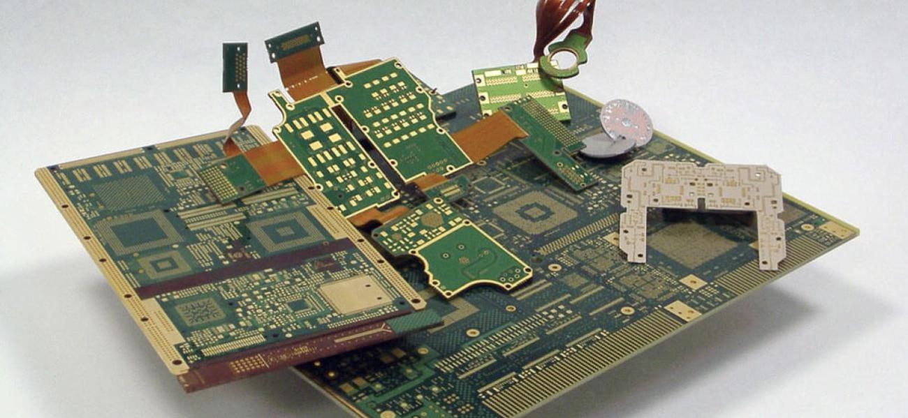
In PCB market, HDI technology required the adoption of new technical skills, new machineries and the implementation of the related production processes including that of filling the through holes and laser holes, necessary for the realization of" filled and capped vias”, technique also known as "plating over filled vias” well described by the IPC 4761 standard as Type VII filling.
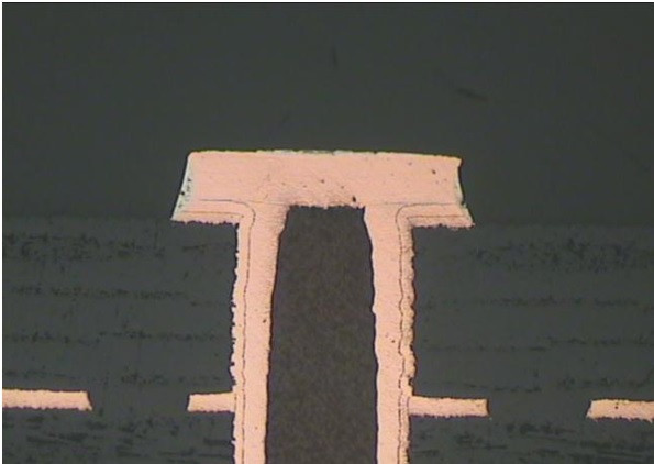
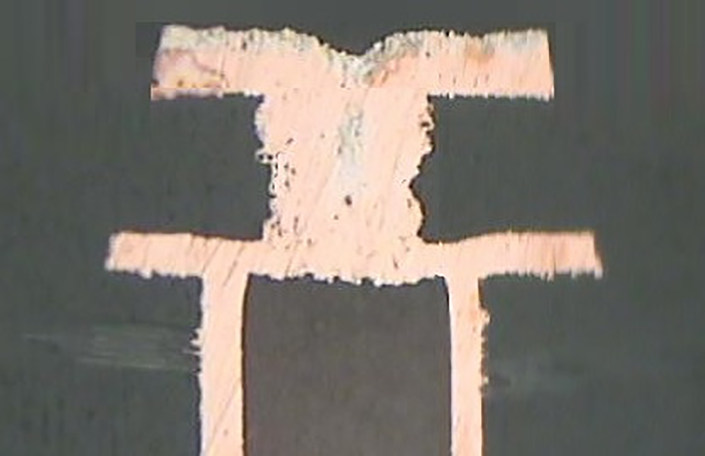
The capped vias technology with hole filling with resin aims to increase the density of the interconnections in printed circuit boards by using the space occupied by through holes as SMD assembly points. This technique consists in filling the holes after plating them, with copper thicknesses on the walls, normally >25µm, and, in any case, defined with the customer.
The resins adopted for "filled and capped vias” have specific insulation properties and dimensional variation with temperatures, they are treated with heat for the relative polymerization and consequent hardening, and, subsequently, are first planarized and then covered with a layer of copper with a thickness of at least 15µm.
This technique can be applied for the realization of different types of printed circuits and with multiple application variants which for this reason are in strong expansion:
- pads used for µBGA, "ball on via technology" and SMD assembly: "Via in Pad Assembly Technology"
- pads used as test points, "Via in Pad Test Technology”
- heat dissipation pads under the cases of the components for "heat management”
- SBU - "sequential build up" construction with laser stacked holes on buried holes treated as capped vias
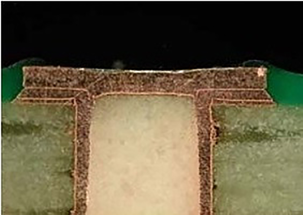
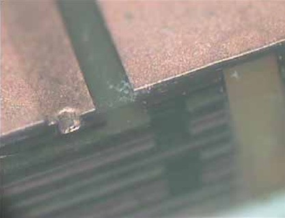
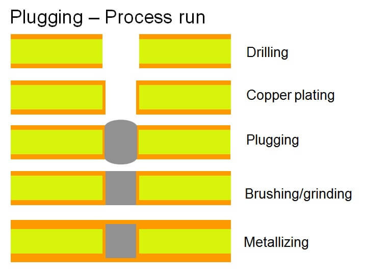
The fundamental operations for filling the holes with resin are carried out in two distinct phases: in the first, the holes are filled with variable pressure and vacuum to allow perfect filling of the holes without the risk of gaps in the resin, while, in the second phase, a surface cleaning of the panel is performed to eliminate the excess resin, facilitating its subsequent planarization.
Whatever the final technology chosen, after complete polymerization, the resin is removed by a mechanical brushing action, called planarization, which can be performed with specific machines that work with cup brushes or with horizontal brushing machines.
The target is to remove the excess resin and create a uniform surface: this operation is a prerequisite for the subsequent over-plating of the filled vias with copper to allow ideal soldering of electronic components. (inserisci disegno).
The knowledge of "capped vias" technology is fundamental today to create compliant pcbs to market and regulations standards required, especially relating to the growing HDI technology demand.